 Int'L Trading Co.,Ltd.")
English
- English
- Español
- Português
- русский
- Français
- 日本語
- Deutsch
- tiếng Việt
- Italiano
- Nederlands
- ภาษาไทย
- Polski
- 한국어
- Svenska
- magyar
- Malay
- বাংলা ভাষার
- Dansk
- Suomi
- हिन्दी
- Pilipino
- Türkçe
- Gaeilge
- العربية
- Indonesia
- Norsk
- تمل
- český
- ελληνικά
- український
- Javanese
- فارسی
- தமிழ்
- తెలుగు
- नेपाली
- Burmese
- български
- ລາວ
- Latine
- Қазақша
- Euskal
- Azərbaycan
- Slovenský jazyk
- Македонски
- Lietuvos
- Eesti Keel
- Română
- Slovenski
- मराठी
- Srpski језик


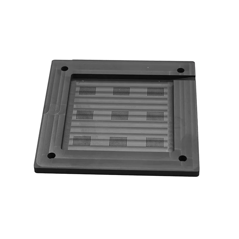
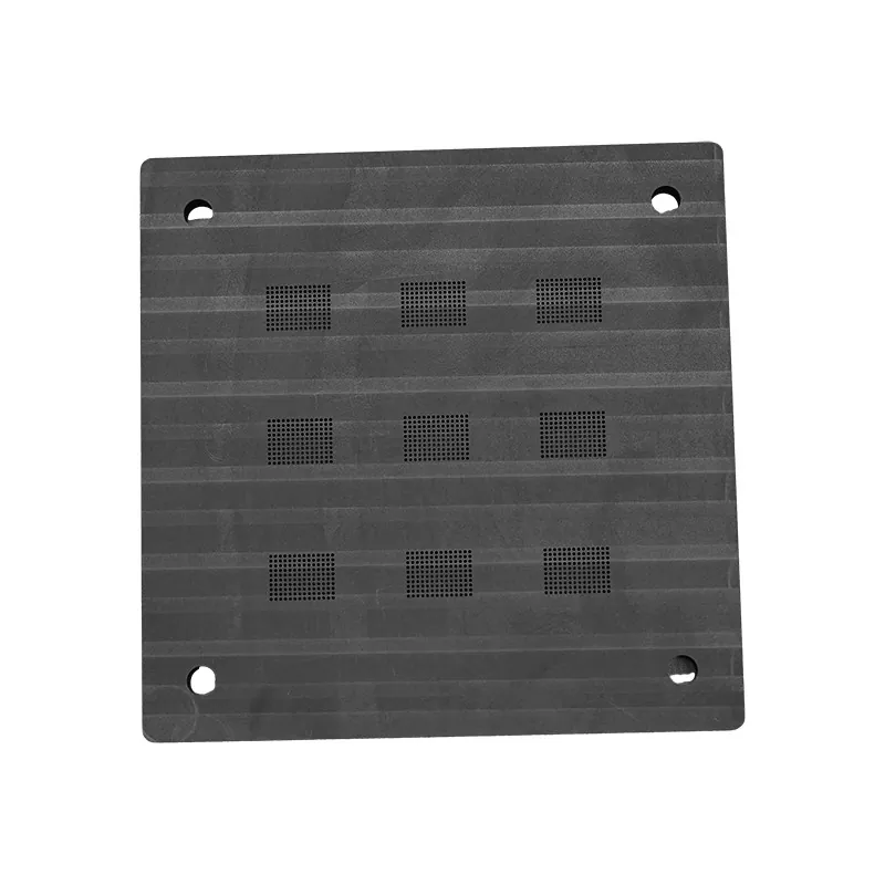
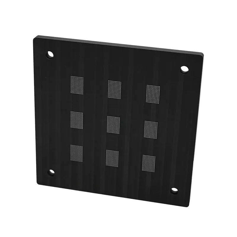
Graphite Ball Placement Fixtures
SIKAIDA Graphite Ball Placement Fixtures systems are high-precision solutions for the semiconductor packaging, electronics manufacturing, and precision instrument industries. Utilizing high-purity graphite and precision machining processes, they meet advanced packaging requirements. As a leading semiconductor tooling manufacturer in China, we provide high-quality customized solutions to global customers, improving production efficiency and product yield.
SIKAIDA Graphite Ball Placement Fixtures employ high-purity graphite and precision machining and surface treatment technologies, meeting semiconductor-grade standards. The surface is smooth and clean, with stable high-temperature performance. The optimized structure facilitates operation and maintenance, effectively improving ball placement efficiency and yield.
High-purity graphite is thermally conductive and corrosion-resistant, ensuring dimensional stability during high-temperature soldering and preventing harmful ion contamination. Special surface treatments guarantee excellent wettability with solder balls, avoiding oxidation contamination.
Technical Specifications
|
Item |
Specification |
Technical Index |
|
Base Material |
High purity graphite |
Purity ≥99.5%, Ash ≤0.5% |
|
Density |
1.7–1.9 g/cm³ |
±0.05 g/cm³ |
|
Surface Flatness |
Precision lapped |
Flatness ≤0.002 mm/m |
|
Surface Roughness |
Ultra smooth |
Ra ≤ 0.4 μm |
|
Operating Temp |
-40°C to 300°C |
Wide temperature range |
|
Ball Position Accuracy |
Diameter ±0.025 mm; Pitch ±0.05 mm |
High precision positioning |
|
Metal Impurities |
Fe ≤10 ppm, Cu ≤5 ppm |
Semiconductor grade purity |
|
CTE (25–200°C) |
4–6 ×10⁻⁶/K |
Matches silicon wafers |
|
Compressive Strength |
≥35 MPa @20°C |
High mechanical strength |
|
Resistivity |
8–15 μΩ·m @25°C |
Stable electrical property |
|
Machining |
5 axis CNC |
Positioning accuracy ±0.01 mm |
|
Surface Treatment |
Vacuum heat treatment |
Stress relief annealing |
|
Standard Size |
100×100×10 mm to 300×300×50 mm |
Multiple standard models |
|
Customization |
Non standard |
Customizable per drawing |
Key Features
Graphite Ball Placement Fixtures boast several key features: 1) High purity (graphite ≥99.5%, free of ion contamination); 2) High flatness (flatness ≤0.002 mm/m, Ra≤0.4 μm); 3) Micron-level ball placement precision (ball diameter ±0.025 mm, ball spacing ±0.05 mm); 4) High temperature resistance (stable performance at 300°C); 5) Excellent thermal management (uniform thermal conductivity, reducing thermal stress).
Application Scenarios
Graphite Ball Placement Fixtures are widely used in semiconductor packaging (high-density packaging such as BGA and CSP), microelectronic assembly (small components such as 0402 and 0201), optoelectronic devices (LEDs, lasers), MEMS devices, and power semiconductors (IGBTs, MOSFETs).
Key Advantages
1. Material Purity Advantage: Low impurity content, low gas evolution rate, chemical stability, consistent batch performance, and compliance with semiconductor industry standards.
2. Precision Advantages: Micron-level flatness and positioning accuracy, smooth and defect-free surface, excellent repeatability in mass production, and adaptability to high-density packaging.
3. Thermal Performance Advantages: Wide operating temperature range (-40°C to 300°C), thermal expansion coefficient compatible with silicon wafers, good thermal conductivity, and stable thermal cycling performance.
4. Process Compatibility Advantages: Graphite Ball Placement Fixtures are compatible with various solders, have a wide process window, are easy to clean, have a long lifespan, and offer significant economic benefits.
Technical Capabilities
The company boasts strong technical capabilities: strict material control, with multiple inspections upon arrival; equipped with a full set of high-precision processing equipment to ensure surface quality; diverse surface treatment processes to meet different needs; a precise testing system to ensure stable accuracy; and products that have passed rigorous environmental testing to adapt to actual production.
Frequently Asked Questions:
Q1: Why choose graphite material for ball placement fixtures?
A1: Graphite material has extremely high purity, excellent thermal conductivity and high-temperature resistance, and is chemically stable in semiconductor processes. Compared to other materials, graphite does not release harmful impurity ions to chips and maintains dimensional stability at high temperatures, making it an ideal material for semiconductor ball placement fixtures.
Q2: What are the specific surface flatness and roughness of the fixture?
A2: Our Graphite Ball Placement Fixtures have a surface flatness controlled within 0.002 mm/m and a surface roughness Ra≤0.4 μm. This extremely high surface flatness and smoothness ensures uniform contact with the chip and substrate, avoiding ball placement defects caused by surface unevenness.
Q3: What is the ball placement accuracy that can be achieved?
A3: Our fixtures achieve a ball placement positioning accuracy of ±0.025 mm and a ball pitch accuracy of ±0.05 mm. This level of accuracy fully meets the requirements of current mainstream semiconductor packaging processes and can handle high-density, micro-pitch ball placement applications.
Q4: What is the maximum operating temperature of the fixture?
A4: Our Graphite Ball Placement Fixtures can operate normally within a temperature range of -40°C to 300°C. This temperature range covers all critical stages of semiconductor packaging processes, including reflow soldering and high-temperature storage.
Q5: Can you provide customized tooling products?
A5: Yes, we can provide customized services according to specific customer needs. Customers can provide detailed drawings or samples, and we can process various non-standard tooling products. The minimum processing size is 0.5 mm, and the tolerance can be controlled within ±0.01 mm.
Q6: What is the service life and reusability of the tooling?
A6: Under normal use and proper maintenance, our graphite ball-mounting tooling can be reused more than 100 times. The actual service life depends on specific usage conditions, process parameters, and maintenance. We recommend regular surface inspection and performance testing to ensure the tooling is in good condition.
Q7: How do you ensure the cleanliness and contamination-free nature of the tooling?
A7: Our tooling undergoes rigorous cleaning and surface treatment after processing, including ultrasonic cleaning, deionized water rinsing, and high-temperature baking. The tooling is packaged in anti-static and dustproof packaging to ensure cleanliness during transportation and storage. After receiving the product, customers are advised to unpack and use it in a cleanroom environment.
Q8: What are the resistivity and thermal conductivity of the tooling?
A8: Our graphite tooling has a resistivity of 8-15 μΩ·m (at 25°C) and a thermal conductivity of approximately 120-200 W/m·K. These parameters ensure a balanced performance in electrical insulation and thermal management, making it suitable for various semiconductor packaging applications.
Hot Tags: Graphite Ball Placement Fixtures, China, Manufacturer, Supplier, Factory
Related Category
Send Inquiry
Contact Info
-
Address
Fengze Two Avenue, Balitai Industrial Park, Jinnan District, Tianjin City, China
-
Tel
-
E-mail
Welcome to our website! For inquiries about our products or pricelist, please leave your email to us and we will be in touch within 24 hours.


